Low Pass And High Pass Filter Circuits
ADVERTISEMENT
 1
1 2
2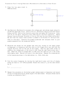 3
3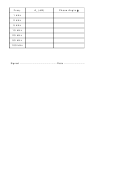 4
4Digital and Interfacing Systems
CENG 215
Lab 5
Low and High Pass Filter Circuits
Name _________________
Objective:
To gain a basic understanding of Low Pass and High Pass RC filter circuits.
Equipment:
1. Scope, function generator, Parts kit
Procedure Part 1:
RC Low Pass Filter
Connect the circuit at right. Apply a 1
1.
kHz sine wave of 2 - 3 V
(with no
PK PK
DC offset) to V
. Connect CH 1 of the
IN
scope to V
and CH 2 to V
.
Set
IN
OUT
CH 1 and CH 2 to AC coupling and
adjust the display until 0 volts is in
the centre of the screen. Use the
Measure mode on the scope to
accurately measure the peak-peak
voltages at V
and V
.
IN
OUT
Select Cursor mode on the scope and measure the time delay (t
) between V
and
2.
d
IN
V
. You can convert your time delay measurement to phase angle with the
OUT
formula:
θ = 360 * Frequency * t
d
Repeat steps 2 and 3 at 2 kHz, 5 kHz, 10 kHz, 20 kHz, 50 kHz and 100 kHz and
3.
record the results in the table below. Voltage gain A
(Linear) is expressed as the
V
ratio of (V
/V
) : A
(dB) is expressed in logarithmic form as 20 log (V
/V
)
OUT
IN
V
OUT
IN
Freq.
V
V
A
(Linear)
A
(dB)
Time delay
Phase
IN
OUT
V
V
t
Angle θ
d
1 kHz
2 kHz
5 kHz
10 kHz
20 kHz
50 kHz
100 kHz
Graph your results using 2 cycle semi-log graph paper. You must use the linear
4.
axis on this graph paper for the voltage gain and the log axis for the frequency
values.
ADVERTISEMENT
0 votes
Related Articles
Related forms


 Tax Deferral For Low-income And Low-income Senior Property Owners Application - Goverment Of The District Of Columbia
Legal
Tax Deferral For Low-income And Low-income Senior Property Owners Application - Goverment Of The District Of Columbia
Legal
 Supplemental Petition To Modify Parental Responsibility, Visitation, Or Parenting Plan/time-sharing Schedule And Other Relief - Florida Circuit Court
Legal
Supplemental Petition To Modify Parental Responsibility, Visitation, Or Parenting Plan/time-sharing Schedule And Other Relief - Florida Circuit Court
Legal

 Form 50-264 - Supplemental Application For Community Housing Development Organization Improving Property For Low-income And Moderate-income Housing Property Tax Exemption Previously Exempt In 2003
Financial
Form 50-264 - Supplemental Application For Community Housing Development Organization Improving Property For Low-income And Moderate-income Housing Property Tax Exemption Previously Exempt In 2003
Financial


Related Categories
Parent category: Miscellaneous